
Peer-Reviewed Publications
Explore selected peer-reviewed journal publications and scientific research results from AdMOS.
All Articles
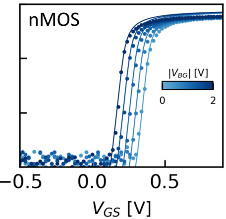
Cryogenic-Aware EDA-Compatible Design Libraries for FD-SOI Transistors
Extending existing FD-SOI foundry libraries with temperature- and back-bias-dependent effects for seamless integration into established EDA design flows.
Read ►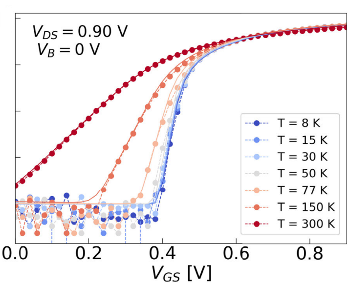
Evaluation of Cryogenic Model Libraries for FDSOI CMOS Transistors
A cryogenic simulation library for FDSOI transistors enabling accurate device- and circuit-level modeling from 8 K to room temperature.
Read ►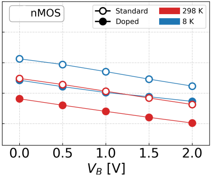
Cryogenic Performance Assessment of FD-SOI Transistors with Counter-Doped Channel
We explore counterdoping as a potential strategy to mitigate the increased threshold voltage at cryogenic temperatures, aiming to reduce power consumption.
Read ►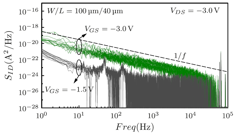
Compact model for the bias-depended low-frequency noise in organic thin-film transistors due to carrier-number and mobility-fluctuation effects
Combines carrier-number and mobility fluctuations in a charge-based compact noise model, validated using organic TFT measurements on flexible substrates.
Read ►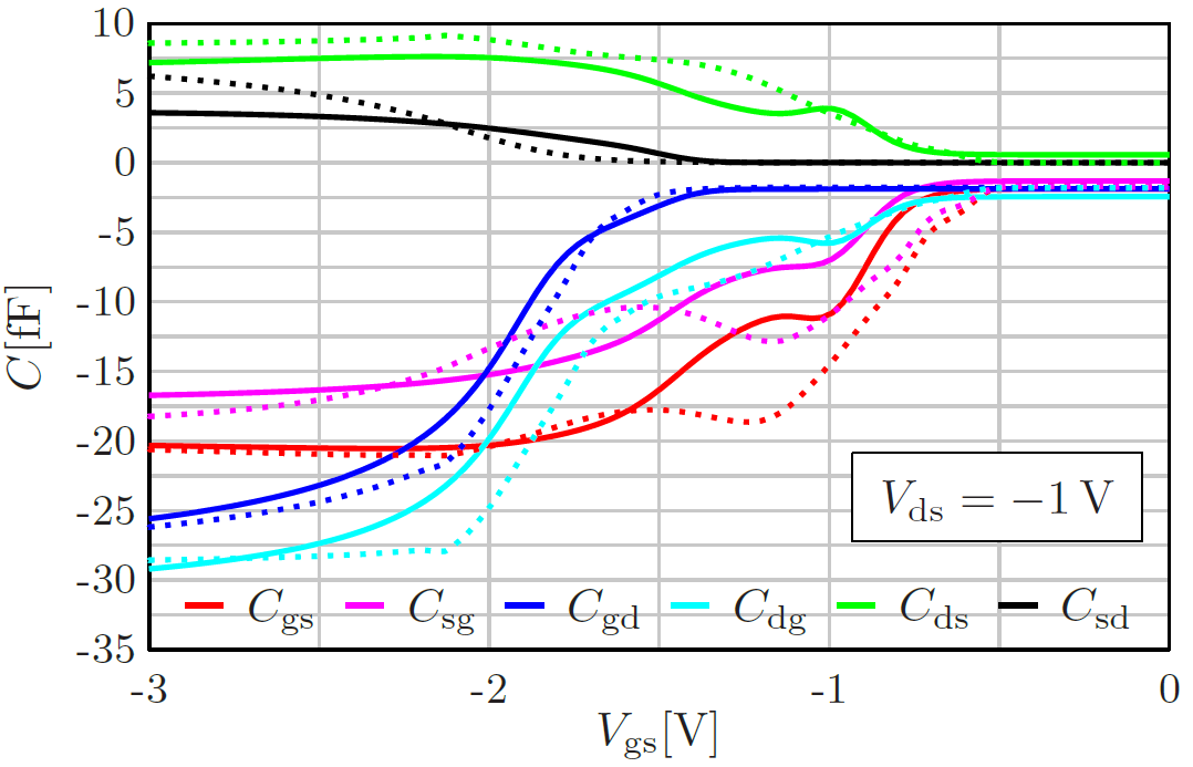
THM-OTFT: A Complete Physics-Based Verilog-A Compact Model for Short-Channel Organic Thin-Film Transistors
Presents a comprehensive physics-based Verilog-A compact model for short-channel organic thin-film transistors, validated using measured device characteristics.
Read ►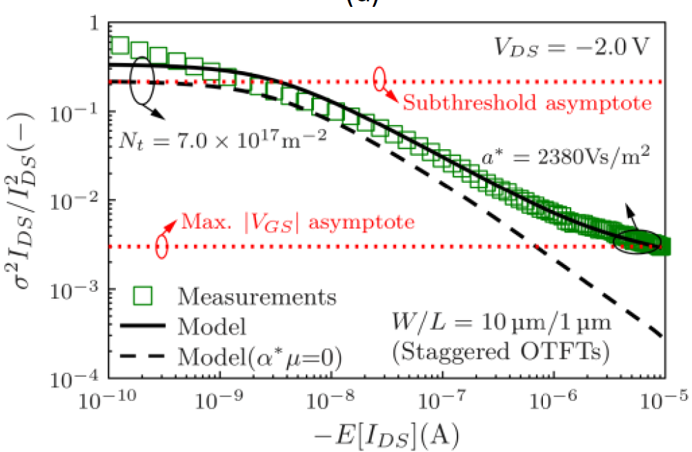
New Compact Modeling Solutions for Organic and Amorphous Oxide TFTs
Reviews physics-based compact models for organic and oxide TFTs, covering charge transport, trapping, stress, capacitances, noise, and circuit simulation.
Read ►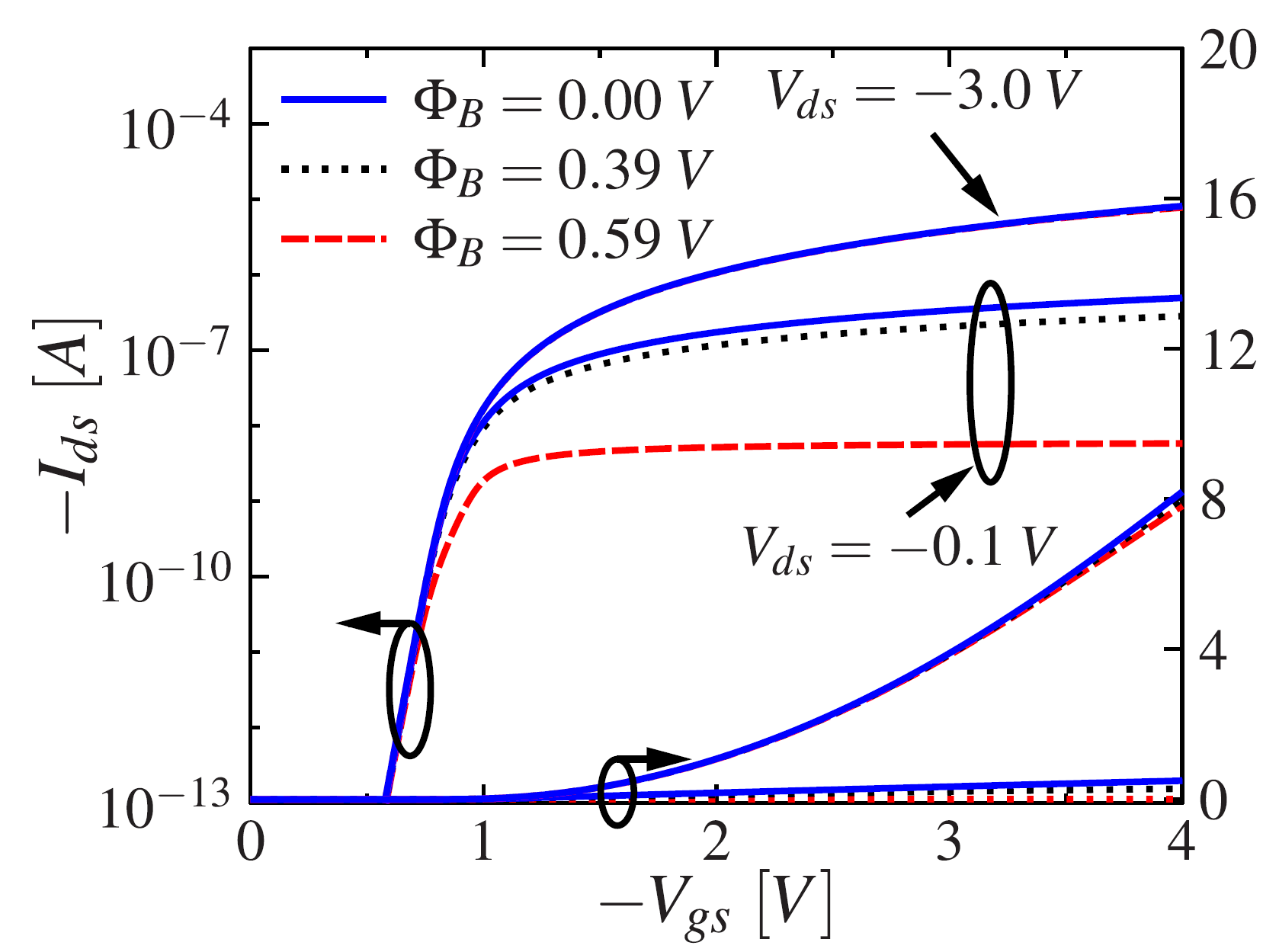
Compact Modeling of Nonlinear Contact Effects in Short-Channel Coplanar and Staggered Organic Thin-Film Transistors
Introduces compact Schottky-contact barrier models that capture nonlinear source and drain contact effects in short-channel organic TFTs.
Read ►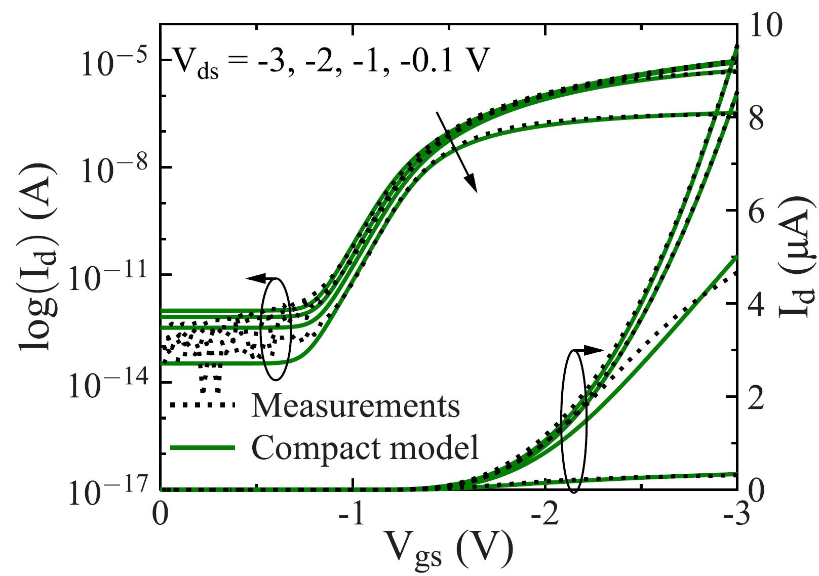
Compact Modeling of Short-Channel Effects in Staggered Organic Thin-Film Transistors
Develops physics-based compact models for subthreshold degradation, threshold roll-off, and drain-induced barrier lowering in short-channel organic TFTs.
Read ►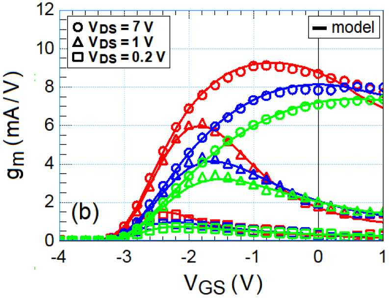
Validation of the Industry-Standard ASM-GaN Model for Gate-Length Scaling
Validates the ASM-GaN compact model against pulsed I-V measurements of AlGaN/GaN HEMTs with different gate lengths.
Read ►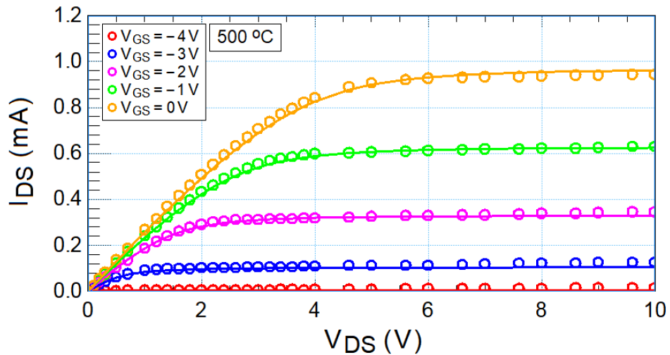
Extreme Temperature Modeling of AlGaN/GaN HEMTs
Enhances the ASM-GaN compact model to capture GaN HEMT current-voltage behavior and trapping effects at temperatures up to 500 °C.
Read ►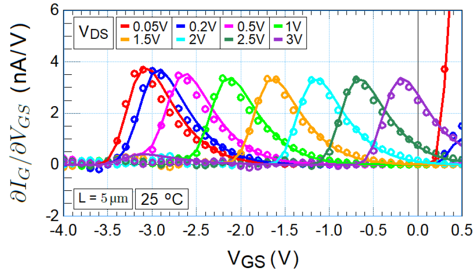
Consistent Surface-Potential-Based Modeling of Drain and Gate Currents in AlGaN/GaN HEMTs
Extends the ASM-GaN compact model with consistent drain- and gate-current descriptions, including key leakage mechanisms across voltage and temperature.
Read ►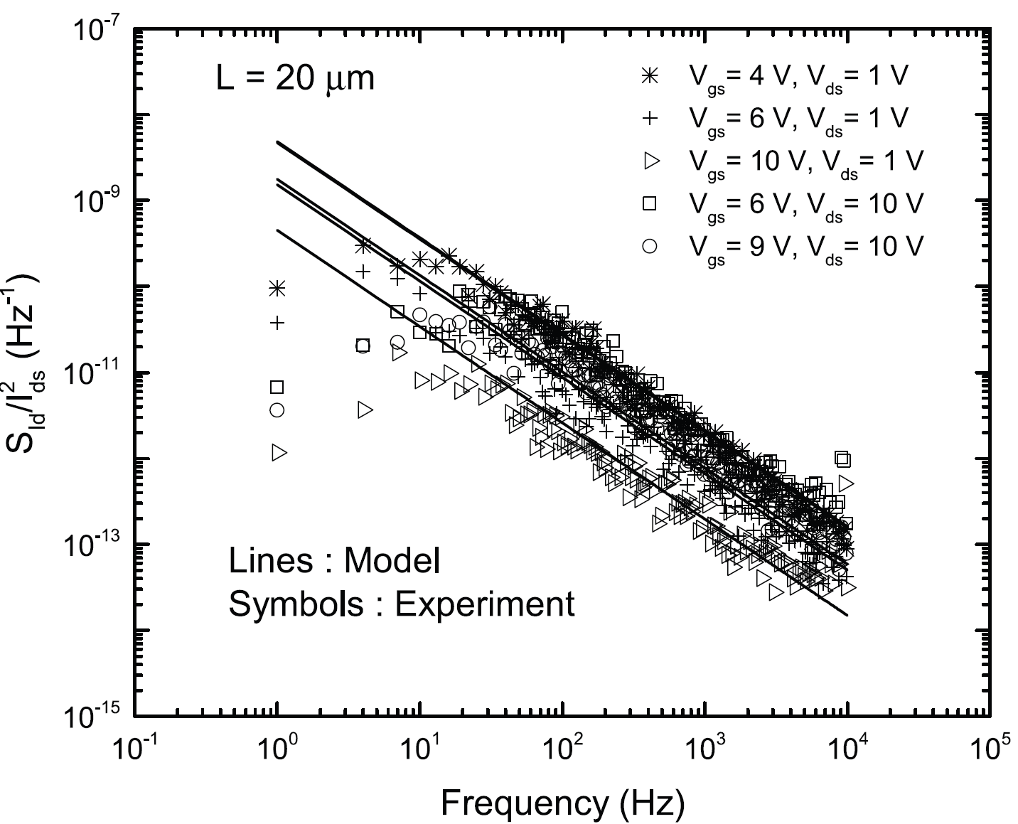
Parameter Extraction and Compact Modeling of 1/f Noise for Amorphous ESL IGZO TFTs
Characterizes and models flicker noise in amorphous IGZO thin-film transistors using unified parameter extraction and noise-model validation.
Read ►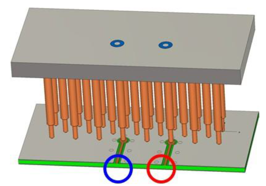
Evaluation of a Spring Probe Card Solution for 5G WLCSP Applications
Evaluates spring-probe-card architectures for 5G wafer-level chip-scale packaging using 3D electromagnetic simulations of millimeter-wave probing structures.
Read ►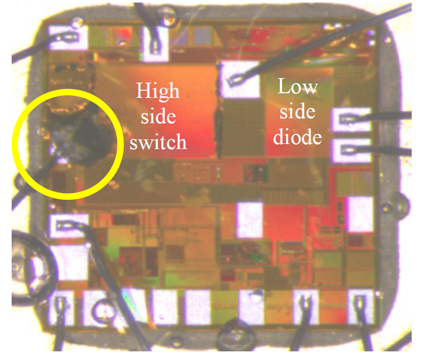
Towards Automatic Diagnosis of Minority Carriers Propagation Problems in HV/HT Automotive Smart Power ICs
Presents an automated substrate parasitic extraction methodology to diagnose minority-carrier coupling and latch-up risks in high-voltage automotive smart power ICs.
Read ►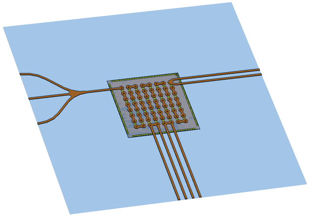
Innovative solutions for systems based on embedding of thin components into flexible printed circuit boards
Presents approaches to embedding ultra-thin flexible silicon chips into polymer-based circuit boards, addressing bending reliability, handling, and assembly challenges in system-in-foil applications.
Read ►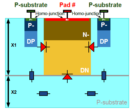
A CAD Integrated Solution of Substrate Modeling for Industrial IC Design
Presents a CAD-integrated substrate-modeling approach for smart-power ICs to predict parasitic coupling between switching power stages and sensitive circuits.
Read ►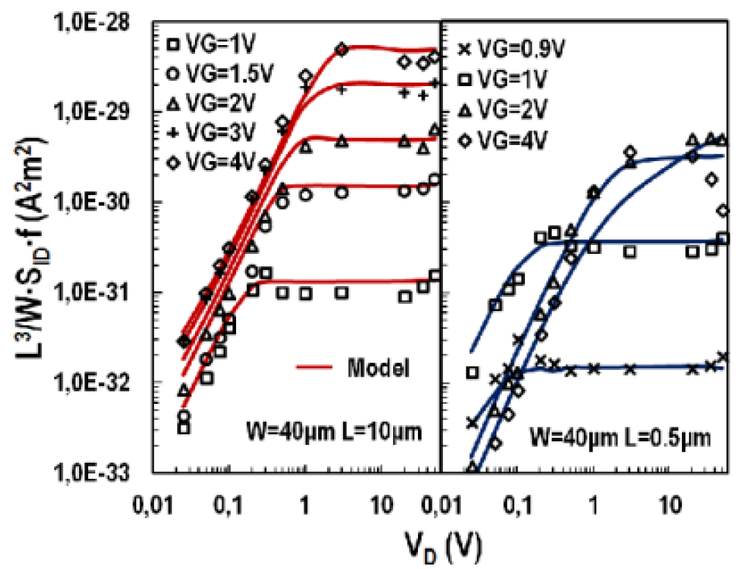
Analysis of Drain Bias Dependence of 1/f Noise in HV-MOSFETs
Examines drain-bias-dependent flicker noise in high-voltage N- and P-MOSFETs, distinguishing channel and drift-region contributions across operating regimes.
Read ►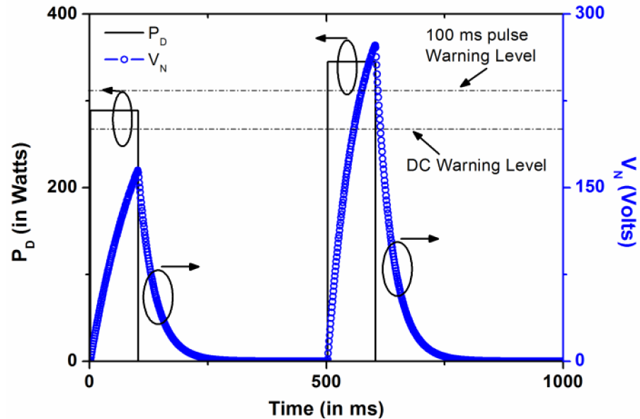
Modeling and Simulation Methodology for SOA-Aware Circuit Design in DC and Pulsed-Mode Operation of HV MOSFETs
Presents a methodology for modeling the safe operating area of high-voltage MOSFETs under DC and pulsed conditions to support reliable circuit design.
Read ►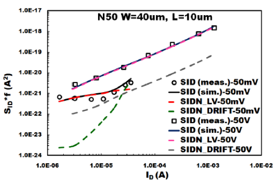
Measurement and Compact Modeling of 1/f Noise in HV-MOSFETs
Characterizes flicker noise in high-voltage MOSFETs over a broad range of biases and validates a physics-based compact model covering channel and drift-region noise.
Read ►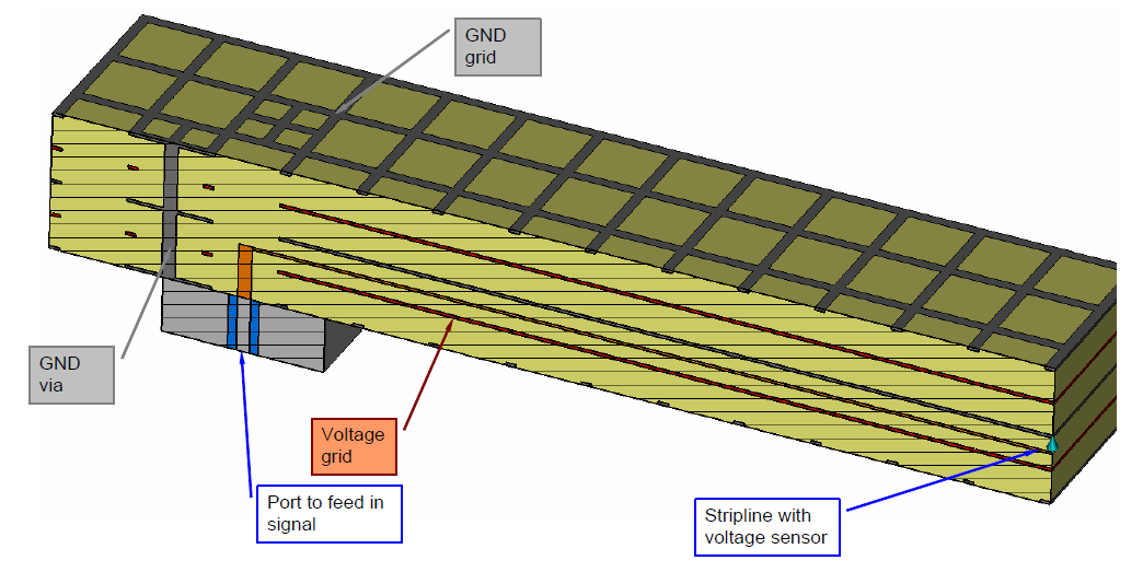
Effects of Partially Broken HF Signal Return on Different Packaging Levels
Investigates how disruptions in high-frequency signal return paths affect electromagnetic coupling and signal integrity across different packaging levels.
Read ►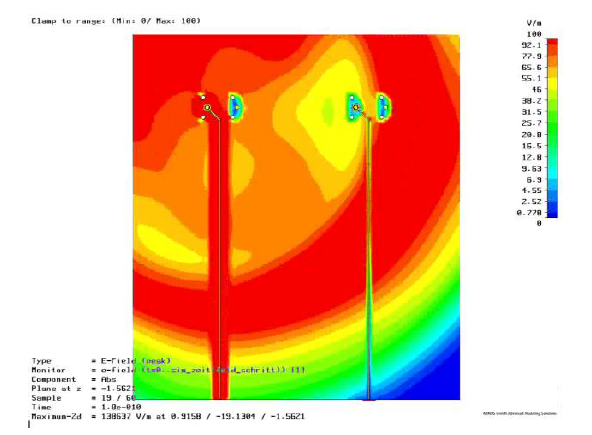
Long Range Connector Via Coupling Effects for High Speed Signals
Investigates long-range coupling between connector vias using 3D electromagnetic simulations and time-domain measurements, highlighting its impact on high-speed signal integrity.
Read ►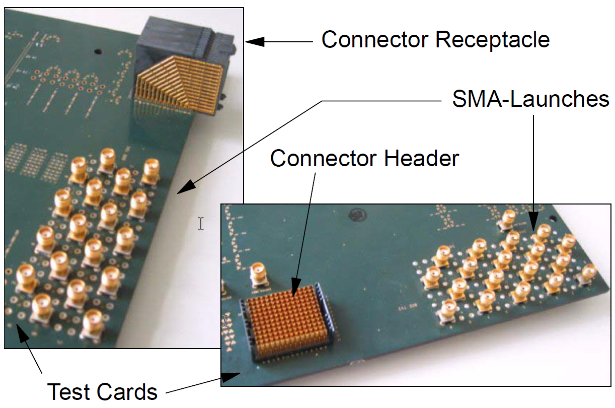
Issues and challenges of Gbps backplane connector characterization
Characterization of gigabit backplane connectors through 3D electromagnetic simulations, measurements, and de-embedding techniques, highlighting the impact of connector footprints on signal integrity.
Read ►